Remote FPGA to FPGA communication
The Ethernet part of the MEEP Shell provides direct capabilities of IP-based connection for EA (Emulated Accelerator). This extends the idea of self-hosted accelerators, controlled by built-in Scalar CPU(s) which are RISC-V based in case of ‘ACME’ with running a Operating System on top of them. The essential part of such functioning becomes the presence of IP connection to satisfy requirements for standard external connectivity in case the Scalar CPU needs it besides the internal NoC connectivity.
MEEP Shell TCP/IP communication: Ethernet
The Ethernet part of the MEEP Shell utilizes hardware resources provided on the Alveo U280 board for external connectivity. They are:
- A pair of board-level QSFP+ optical units each having bandwidth of up-to (28 Gb/s x 4 lanes) = 112 Gb/s.
- A set of FPGA-level Ultrascale+ GTY transceivers having a bandwidth of up-to 32.75 Gb/s per external differential pins pair.
GTY transceivers are connected as differential quads to 4 lanes of each of QSFP+ connectors, thus utilizing their full bandwidth. Ultrascale+ GTY transceiver is FPGA hard SerDes solution present automatically in a set of interface IPs provided by Xilinx. Among them, there are PCIe endpoint, Aurora interface, Ethernet related cores.
Xilinx provides a bunch of Ethernet IPs related to different generations of Ethernet standards starting from 10Mb/s to the latest 400Gb/s [XIP]. All of them present separate or combined 2 levels of implementation:
- Physical layer or PHY, which includes mentioned above built-in GT transceivers.
- Media Access Controller or MAC implemented in regular FPGA logic fabric.
PHY level is always free of charge opposite to MAC level which in most cases requires separate licensing from Xilinx. At the same time, third-party MAC IPs are available on the market including open-source ones. For some Ethernet IPs Xilinx provides SW drivers mitigating the development of application software.
The following UltraScale+ Integrated 100G Ethernet Subsystem [100GIP] is chosen as the basis for the MEEP Shell Ethernet part. It includes both PHY and MAC levels requiring just no-charge license for MAC and is able to utilize close to maximum bandwidth allowed by U280 hardware. But no software driver layer and examples are provided for it from Xilinx.
In order to provide Ethernet capabilities for EA, a kind of full Ethernet Controller solution is required. As it is assumed to be connected to a CPU inside EA (primarily RISC-V based) both hardware implementation and software support should be provided. Generally Xilinx doesn't provide any full solution for such a kind of Ethernet Controller. But some software examples are provided implementing different aspects of IP-connection applications and assuming some set of hardware used.
Besides PHY and MAC layers, another essential part required for a full Ethernet Controller solution is the DMA engine. It allows to transmiting and receiving data at full protocol speed not involving EA CPU for that purpose.
The simplified block diagram of Ethernet Controller as part of the MEEP Shell is presented in Figure 1 as follows:
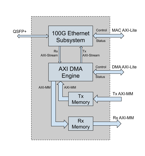
The design of Ethernet Controller consists of four main parts:
- Xilinx UltraScale+ Integrated 100G Ethernet Subsystem.
- Xilinx AXI DMA Engine [XDMA].
- Transmit data memory.
- Receive data memory.
Ethernet Prototype Design
The Ethernet solution is fully based on independent prototype design. It provides debugged hardware for instantiating in MEEP Shell and hardware-specific software layer for further integration with standard network IP-based protocols on EA CPU side.
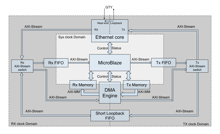
The simplified block diagram of the design is presented below in Figure 2:
.
MicroBlaze as a soft CPU core from Xilinx, plays the role of EA CPU. It provides the ability to debug all hardware specific control of the Ethernet solution. Besides the control features, it is able to provide direct data streaming via built-in Fast Simplex Links (FSL) thus helping in separate debugging and diagnostics of parts of the design.
From the Ethernet core side data streaming in both directions is provided by 512-bit wide Tx and Rx AXI4-Stream interfaces operating at 322.266 MHz. Therefore, all the rest of parts of the design have the same streaming properties.
Besides the MicroBlaze, the main originator of Tx data and acceptor of Rx data present in the design is a DMA engine accompanied with its corresponding Tx and Rx memories. Xilinx AXI DMA core able to convert AXI4-Stream input/output to AXI4-MM write/read accesses is used for that purpose. The width of AXI4-MM interfaces is intentionally the same 512 bits (64 bytes) as for AXI4-Streams to exclude any stalls due to width conversion.
Short Loopback implements the feature of data loopback with bypass of the Ethernet core and serves the purpose of checking the test infrastructure itself and debugging the test software. At the same time, it already uses clocks generated by Tx and Rx parts of the core and thus at least checks that these clocks are up and running, confirming that the basic wiring of the Ethernet core is done correctly.
Finally, the design contains all kinds of connections for AXI4-Stream links allowing to debug and characterize data streaming separately for different units. They may be sorted as follows:
- Tx stream originator options: MicroBlaze/DMA.
- Tx stream acceptor options: Ethernet core/Short Loopback.
- Rx stream originator options: Ethernet core/Short Loopback.
- Rx stream acceptor options: MicroBlaze/DMA.
Few specifics of AXI4-Stream behavior for the 100Gb Ethernet core compared with the standard one were discovered. They relate to side-channel signals serving the purpose of controlling data stream flow. Essentially utilized side-channel signals are: TREADY, TVALID, TLAST, TKEEP. The standard designation of these signals is the following:
- TREADY / TVALID pair provide every word hand-shake signalling.
- TLAST allows the user to cut the stream to packets by marking the last word in a packet.
- TKEEP vector allows having not full words by marking valid bytes.
The confirmed in 100G Ethernet Subsystem Product Guide [100Guide] differences to the above behavior are the following:
- No suspending of a packet transmission is possible by deassertion of TVALID signal in TX AXI4-Stream interface (otherwise underflow condition happens).
- No suspending of a packet reception is possible by deassertion of TREADY signal in RX AXI4-Stream interface (otherwise overflow condition happens).
- No designation of valid bytes is possible by TKEEP vector in packet words besides the last one (accompanied by TLAST signal) in both TX and RX AXI4-Stream interfaces.
As the DMA engine utilizes the same signals to control stream flow in a standard manner, in order to limit their usage according to above rules the proper alignment of memory allocations for DMA transfers was applied and checked in the tests described below.
Functionally, 3 clock domains are present in the design:
- MicroBlaze system clock domain (100 MHz).
- Ethernet Tx clock domain (322.266 MHz).
- Ethernet Rx clock domain (322.266 MHz).
CDC (clock domain crossings) along data paths are implemented inside the following units:
- Tx FIFO/DMA Tx memory for System clock to Tx clock CDC.
- Rx FIFO/DMA Rx memory for Rx clock to System clock CDC.
- Short Loopback FIFO for Tx clock to Rx clock CDC.
Test Application
Bare-metal test application running in MicroBlaze provides self-diagnostic of the parts of the design, testing of all essential functioning modes and data exchange characterization. Three test functioning modes are implemented and may be chosen in prompt menu of the application:
- Single-Board Loopback diagnostic tests.
- Two-Boards Communication diagnostic tests.
- Two-Boards IP-based tests.
Single-Board loopback diagnostic tests
The Loopback tests are executed in two essential sub-modes:
- Short loopback.
- Near-end loopback.
The first one serves for checking test infrastructure itself not involving the datapass through the Ethernet core. In this sub-mode, the upper limit of AXI4-Stream interface bandwidth is also checked. Its absolute maximum is 512 bits x 322.266 MHz = 165 Gb/s. Being measured when DMA is used as both source and acceptor of the full amount of Tx/Rx memories (1 MB each) the achieved speed is some above 141 Gb/s. Not reaching the absolute limit is explained by overheads due to the following few factors:
- Resynchronization stage is still present between Tx and Rx domains as Short Loopback FIFO thus providing additional latency.
- In spite of DMA AXI-MM interfaces being clock and width aligned with AXI-Stream ones, AXI-MM bursts are still limited in length (max available length 64x512-bit words is set in AXI DMA IP).
- Software-activated start and stop of AXI Timer while making DMA Tx/Rx transfers kick-off.
Also, the size and the number of transfers programmed in a DMA affect the measured speed. The fewer the number of transfers and the bigger their size is, the higher speed is measured. Therefore, the best result may be achieved when one big DMA transfer is done.
The second sub-mode conveys data via the whole Ethernet core up-to GTY Tx and Rx ports, which are connected to each other in this mode. Thus the data pass up-to physical connection is tested in this sub-mode still not involving the second board.
Two-Boards communication diagnostic tests
These tests check all parts of the design in different modes on two boards involving real exchange of test data between them. The boards synchronize automatically and exchange with a bunch of data packets verifying them. The communication between DMA engines is done in two ways:
- Asynchronous exchange.
- Round-trip exchange.
In the first case, both sides independently send and receive data thus checking full-duplex abilities of the connection.
In the second case, two sides play correspondingly "Initiator" and "Responder" roles. This case provides mostly true measurement of the transfer speed being done on the "Initiator" side. The measurement done for this communication shows the result 27 Gb/s. Here the same factors as mentioned above for DMA Short Loopback test play as overheads decreasing specified bandwidth of 100Gb Ethernet core. In addition to those limitations, at least the following ones affect too:
- Met issue of inability to make a single DMA kick-off for a bunch of Tx transfers thus requiring software to do separate DMA kick-off for every transmitted packet.
- The maximum packet length available for 100Gb Ethernet core to be set in Vivado is 9600 bytes (practically confirmed maximum is 9596 bytes).
Two-Boards IP-based tests
These tests implement real Internet Protocol data exchange:
- ICMP (Internet Control Message Protocol) packets exchange on the basis of PING command.
- UDP (User Datagram Protocol) packets exchange.
- TCP (Transmission Control Protocol) packets exchange.
All these tests are based on software examples from Xilinx. The initialization of 100Gb Ethernet core and setup of two-boards connection is implemented outside the tests themselves. The procedure is done in the same way as for Two-Boards communication diagnostic tests.
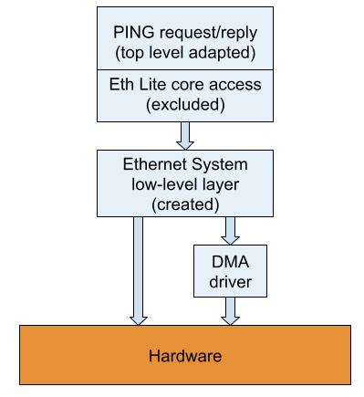
ICMP test is based on "Ping request" and "Ping reply" examples provided for AXI Ethernet Lite MAC core. Top level of examples is adapted to make them a part of the test application. Internally, the examples implement all protocol related actions which are based on accesses to the Ethernet-Lite core driver. All such accesses are replaced with accesses to the own newly created hardware layer. This layer is presented as a class where all hardware related definitions and methods are collected. Regarding the DMA engine it uses access to the AXI DMA core driver by Xilinx.
The structure of PING test is presented in Figure 3 below:
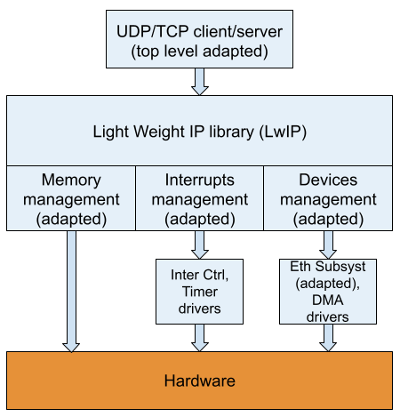
UDP/TCP tests are based on software applications suggested by Vitis if appropriate Xilinx units are present in the hardware platform. Like for PING examples the top level is adapted to make them a part of the test application. Internally, these examples are based on an open-source library for bare-metal applications: LwIP (Lightweight IP). This library contains implementation of standard network IP-based protocols usually already contained in OS software level. The library also contains a middle layer responsible for interaction with hardware. It includes:
- Devices management.
- Interrupts management.
- Memory management.
For all these parts of the middle layer an adaptation was required.
LwIP Devices/Interrupts management adaptation
In part of ‘Devices and Interrupts’ management Xilinx provides its contribution to the LwIP library. The list of four supported Ethernet cores from Xilinx is presented below:
- AXI Ethernet Lite MAC core.
- Tri-Mode Ethernet MAC core.
- AXI 1G/2.5G Ethernet Subsystem core.
- Zynq PS Gigabit Ethernet MAC Controller.
Besides supporting particular Ethernet cores, Xilinx provides their software integration with some of the storage engines. Most of options are provided for AXI 1G/2.5G Ethernet Subsystem:
The AXI 1G/2.5G Ethernet Subsystem being integrated with AXI DMA core was chosen as a unit which is mimicked for the LwIP middle layer instead of actually used 100Gb Ethernet core integrated with the same AXI DMA core.
Below the main changes done in ‘Devices/Interrupts’ management (Xilinx contribution to LwIP) caused by the specifics of the design are listed:
- While setting the length of the transmitted packet for DMA transfer, taking into account that 100Gb Ethernet core is not able to transmit packets less than 64 bytes.
- While receiving the packet taking its length as truly transferred length by means of AXI DMA core driver method instead of extracting it from specific DMA user data field.
- Buffer Descriptors (BD) ring for DMA is allocated in DMA dedicated Scatter-Gather (SG) memory instead of system memory heap.
- While initializing DMA and Interrupt Controller, DMA engine address and DMA Tx/Rx interrupt numbers are taken directly from hardware definitions instead of special config structure for non present AXI 1G/2.5G Ethernet Subsystem.
- Ethernet core error interrupt and corresponding handler are not registered in the Interrupt Controller driver because such interrupt is absent for 100Gb Ethernet core.
LwIP Memory management adaptation
LwIP library has its own ‘Memory’ Management system since it is assumed to function without OS level. It has few options for management of different types of LwIP buffers and LwIP own heap both static and dynamic based.
Below the main changes done in ‘Memory’ management caused by the specifics of the design are listed:
- Default LwIP allocation macro based on system memory heap was overridden by macro with fixed allocations in DMA dedicated Tx and Rx memories for corresponding types of LwIP buffers.
- Allocation alignment set by default to 64 bytes was overridden by setting to a rounded value of maximum packet size (2048 bytes) according to specifics for combined functioning of 100Gb Ethernet core and DMA engine mentioned above.
- Proper configuration of sizes of different buffers was done through available LwIP parameters. They were adjusted from default values in order to satisfy increased memory consumption due to above alignment and still fit to DMA dedicated Tx/Rx memories with saving UDP/TCP tests functionality.
- Disabling spreading of TCP packet over few memory allocations by overriding corresponding default definition in order not to distinct whole packet from its chunk when limiting packet minimum length to 64 bytes while configuring DMA linked BDs.
The structure of UDP/TCP tests is presented in Figure 4:
Conclusion
The presented Ethernet prototype design allows to discover the specifics of hardware cores to be used for MEEP Shell Ethernet solution and their combined functioning, and summarizes the handling of this specifics in test application which implements real data exchange between two boards including Internet Protocol based exchange.
References
[XIP] https://www.xilinx.com/products/technology/ethernet.html
[100GIP] http://www.xilinx.com/products/intellectual-property/cmac_usplus.html
[XMA] https://www.xilinx.com/support/documentation/ip_documentation/axi_dma/v7_1/pg021_axi_dma.pdf
[100Guide] http://www.xilinx.com/support/documentation/ip_documentation/cmac_usplus/v3_1/pg203-cmac-usplus.pdf#page=66
[OVI] Open Vector Interface (September 2020), https://github.com/semidynamics/OpenVectorInterface
Next steps in the near future?
Find more information about MEEP’s ecosystem here.