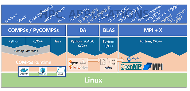
MEEP is a full stack research project that combines SW/HW and SW/HW codesign targeting an FPGA platform that enables large-scale proof of concepts. Below are tables that provide more project details on the HPC Applications, SW toolchain, Emulation Platform and the first Accelerator targeting MEEP.
Each MEEP platform layerhas its own responsibility, and all of them might be analyzed using profiling and performance monitoring tools.
We have identified a suite of potential workloads to accelerate on the MEEP platform:
Emerging bioinformatics applications.
Emerging HPDA (High-Performance Data Analytics) frameworks.
Traditional HPC applications.
As shown from left to right in the figure below, there is a rich set of applications and we will focus on the applications that simultaneously have the most RISC-V ecosystem support and the largest HPC impact.
MEEP software stack
Emerging bioinformatics applications
MEEP will consider in its applications portfolio some of applications and application workflows from different application areas that are developed on top of PyCOMPSs/COMPSs (see the Software Toolchain tab). Some of these are:
Multi-Level Monte Carlo (MLMC) codes.
BioBB library (including GROMACS).
Multiscale Online Nonhydrostatic Atmosphere Chemistry model (NMMB-Monarch).
Dislib ML library, or the SMUFIN code.
Emerging HPDA frameworks and applications
For HPDA, the idea is to mainly use benchmarks (such as the TensorFlow's Official Models and the Spark-Bench), and possibly internal workloads like the AIS-Predict, a TensorFlow application for vessel trajectory prediction. Likewise, we will use Bolt65 suite, a just-in-time video processing software in the HPDA collection.
MEEP will use microkernels (such as DGEMM, SpMV, FFT, and others), representative code hot spots (functions, loops, etc.) to drive the software/hardware co-design aspects of the MEEP accelerator. Our focus in that case is set on the performance-efficiency achieved by low-level optimizations for the efficient exploitation of the architecture.
MPI+X workloads
HPC benchmarks such as HPL (High Performance Linpack).
HPCG (High Performance Conjugate Gradient) and continuing with four widely used HPC applications: Quantum Espresso, Alya, NEMO, and OpenIFS.
The MEEP software stack offers a different perspective about accelerators and which applications can execute efficiently on this hardware. This is also an opportunity to extend these applications into the RISC-V ecosystem, creating a completely open ecosystem from hardware to application software.
Regarding the Operating System (OS), two complementary approaches will be considered to expose the MEEP hardware accelerators to the rest of the software stack:
1) offloading of accelerated kernels from a host device to an accelerator device, similar in spirit to how OpenCL works.
2) natively execute a fully-fledged Linux distribution running on the accelerator that will allow the native execution in the accelerator of most common software components, pushing the accelerator model beyond the traditional offload model explored in the first option.
MEEP's approach will use the following software components:
LLVM is an umbrella project hosted by the LLVM foundation for the development of compilers and related tooling. We will be developing extensions to the LLVM compiler and other essential toolchain components, contributing to a more robust environment.
OpenMP is an industrial standard that defines a parallel programming model based on compiler directives and runtime APIs. The MEEP software stack will use the LLVM OpenMP runtime.
MPI (Message Passing Interface) is a runtime library for parallelization of applications in distributed memory systems, such as clusters, that implements a SPMD (Single Program Multiple Data) paradigm.
PyCOMPSs/COMPSs is a parallel task-based programming model for distributed computing platforms.
TensorFlow is a free and open-source software library for dataflow and differentiable programming across a range of tasks.
Apache Spark (Spark for short) has as its architectural foundation the Resilient Distributed Dataset (RDD), a read-only multiset of data items distributed over a cluster of machines, that is maintained in a fault-tolerant way.
The MEEP project also envisions the usage of containers as the mechanism to package, deploy and offload the execution of applications. However, since the project is based on a new architecture, not all needed software components will be available.
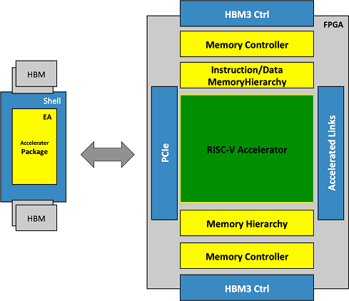
In general, MEEP can leverage the FPGA built-in components and hardware macros, and efficiently map other components (IPs or custom designs) to the available structures of the FPGA. The components in the system are arranged as multiple accelerator cores operating in parallel, and able to execute different kinds of HPC applications.
MEEP extends the traditional accelerator system architecture beyond the traditional CPU-GPU systems by presenting a self-hosted accelerator.
This self-hosted accelerator can increase the number of accelerators “managed” by a traditional host, reducing the host CPU energy tax, boosting the system efficiency.
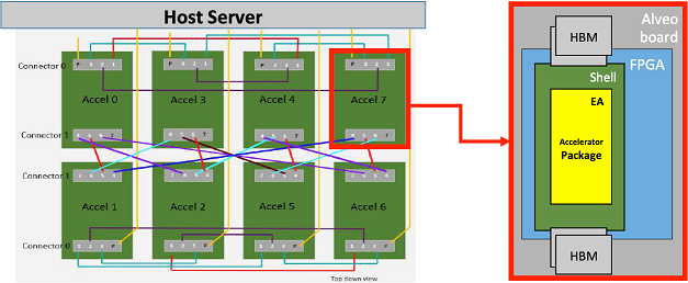
More specifically, the emulation platform architecture might be structured into two well-differentiated parts (below):
The FPGA Shell: This element contains all the necessary mechanisms for the accelerator to communicate with the host, and also with other neighboring accelerators.
The Emulated Accelerator (EA): This element is where all the data processing is executed and involves computation and memory management.
MEEP Targeted UBB board in Phase 2 (image on the left), and a detailed view of the Emulation Platform (image on the right)
Communication infrastructure
As shown above, the host server is connected by PCIe to each of the FPGAs (host interface) and all FPGAs are fully connected with dedicated SerDes (Serializer/Deserializer) links, enabling all-to-all communication between the FPGAs or emulated accelerators.
This communication infrastructure can be exposed to the software layers in a variety of ways, like OpenMP/MPI, etc. Thus, we have software APIs to enable as well as the RTL and IP blocks inside the FPGA to move the bits around. All of these communication options enable a wide variety of EA mappings and system compositions utilizing one or more FPGAs to define a node.
Emulated accelerator architecture
MEEP’s first emulated accelerator architecture is a disaggregated access-execution architecture that allows us to embed more intelligence near the memory controller and, in doing so, select how to use the memory interface.
The key challenge is to combine the knowledge of the larger data structures (vectors), with the application program flow to optimize the use of the on-chip memory hierarchy. Using vectors enables the system to see into the future and orchestrate memory requests in both space and time, providing a glimpse into the future, and optimizing on-chip memory usage.
The emulated accelerator architecture is a scale-down instance of the ACME accelerator, which has the need to communicate with the rest of the system (host, and/or other accelerators in different FPGAs). Here is where the Software Stack and the Hardware Stack come together to provide the required capabilities to the system to be able to run applications.
The following video describes and shows the implemented mechanisms to communicate the current version of the emulated accelerator with the host: Demo.
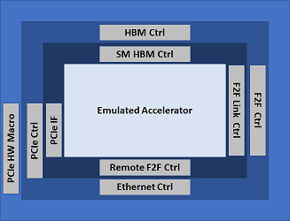
The Shell
Each FPGA in the system will use a standard FPGA shell defined in MEEP, as three distinct layers (below). This FPGA shell is composed of IP blocks common to most FPGA-based systems for communication and access to memory:
PCIe: This IP allows the communication between the host and the FPGA. It provides a universal interconnect to the chip and the system.
HBM: This IP provides fast and high memory capacity to promote a self-hosting accelerator.
F2F: The accelerator links are useful for nearest-neighbor and remote FPGA communication (F2F); inter and intra chiplet data movement.
The innermost concentric ring is the MEEP shell interface to the internal FPGA logic of the emulated accelerator or other FPGA functionality. This ring is MEEP specific RTL that provides a common interface to the remaining FPGA logic. The goal is to keep it as minimal and flexible as possible.
Shell description overview
Current work: Emulation platform architecture-Phase 1
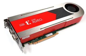
Taking advantage of the latest available FPGA hardware platform, MEEP uses the Alveo U280 [Xilinx-U280], an actively cooled FPGA card, as shown in the figure below. This uses the VU37P FPGA. This FPGA has various hard IP blocks that can be used in the system, including: HBM and related memory controller, PCIe controller and drivers, QSFP and Ethernet functionality. These hard macros align well with some of the base functionality of the ACME EA.
Alveo U280 card
As part of this Phase 1, and having as a final goal the generation of a functional FPGA Shell, the work has been divided into several steps:
(1) characterizing each of the IPs separately: This first step will allow us to understand the requirements and features of each of these IPs and, at the same time, identify the missing pieces that need to be developed in order to fulfil the emulation platform expectations. The following videos shown the progress on them:
HBM. This is a demonstrator of how by exploiting the reordering features of the HBM the performance can be improved.
FPGA to FPGA communication through Ethernet. The video shows the integration of this IP in OpenPiton, as a first approach to the final MEEP solution, and how two U280 boards are able to communicate through it.
If you prefer to read what has been done with the Ethernet IP, do not forget to take a look at the article: 'MEEP Shell - Part 1: The Ethernet IP.'
(2) the FPGA Shell as a composition of all these individual IPs: The objective pursued by this step is to create an IP with clear and clean interfaces to allow the exploitation of these IPs in a seamless way. In an attempt to create functional flavors of an FPGA Shell, the first approach includes the PCIe and the HBM, which are the minimal required IPs to communicate with the host and with the emulation platform (and the inner EA), and to enable the self-hosting features, respectively.
(3) connecting the EA to the FPGA Shell: Here is where the RTL of the accelerator architecture and the FPGA Shell converge to create an emulated accelerator able to interact with the rest of the system (the host and/or other emulated accelerators).
The following video collects the progress of the steps (2) and (3) together. Actually, a more detailed explanation about what is the MEEP FPGA Shell and its real implementation in the emulation platform is shown. Demo: Automatic Shell + EA generation
The self-hosted accelerator conceived in MEEP is envisioned as a collection of chiplets that are composed together in a module. The goal of MEEP is to capture the essential components of one of the chiplets in the FPGA and replicate that instance multiple times.
Although those components might be seen as a collection of different elements, they can be separated into two main categories according to their main functionality: memory or computation (below).
High-level description of the Emulated Accelerator
On one hand, all memory components will be distributed creating a complex memory hierarchy (from HBM and the intelligent memory controllers down to the scratchpads, and L1 caches).
On the other hand, the computational components will be organized into hierarchical layers by following a bottom-up approach, starting at module-level and building on top of that by composition, up to a system-level component. This one can be seen as the computational engine, which will be a RISC-V based accelerator.
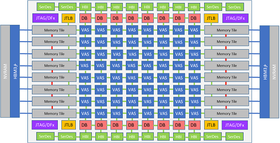
The targeted accelerator in MEEP is called Accelerated Compute and Memory Engines (ACME), and the figure below shows its high-level architecture view with a variety of different blocks.
The figure below shows the high-level ACME architecture with a variety of different major blocks.
The ACME architecture
The ACME architecture component’s details
1. ACME Accelerator in MEEP
The ACME accelerator is composed of two main components: (1) the computational engine, and (2) the memory engine. Both of them are in charge of increasing the performance of the accelerator under different working contexts, since they are developed for specific tasks. On one hand, the computational engine is responsible for operating with the data (scalar and vector elements). On the other hand, the memory engine is responsible for dealing with memory transactions and accesses, with the final purpose of reducing the energy and saving memory accesses.
The table below summarizes the main features to be exploited by the architecture under different working contexts, based on the dominant HPC application characteristic.
Main Component
System-level Architecture
Module-level
Micro architecture
Features
Computational Engine
matrix of
VAS Tiles
1. Scalar core
2. Co-processors
2.1. VPU,
2.2. SA-HEVC
2.3. SA-NN
(Compute-bound applications)
●Specialized accelerators
(VPU, SA-HEVC, SA-NN)
●Common co-processor shell
●ISA upgrade
●Custom instructions
●New interlane interconnect
Memory Engine
matrix of Memory Tiles
1. Two-Level VRF
2. MCPU
3. Flexible L2/L3
4.Memory Controller
(Memory-bandwidth bound applications)
●Streaming Vector Register File
●Real & Virtualized vector length
●Memory operation off-loading
●Flexible memory hierarchy
●Smart memory addressing
●Sparse to dense transformation
●Smart data management
According to the table, the Computational Engine is designed to perform well on the compute-bound applications, whereas the Memory Engine is designed to improve the efficiency for memory-bandwidth bound applications.
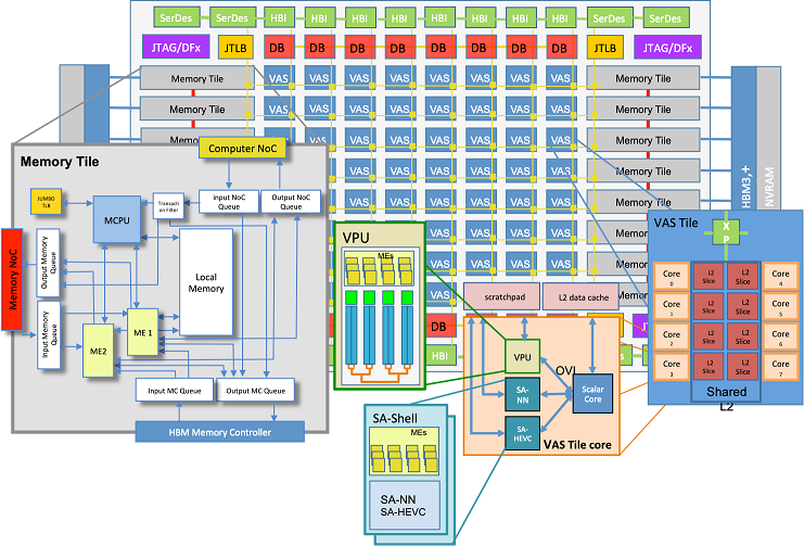
Accelerated computational engine
Each VAS Accelerator Tile is designed as a multi-core RISC-V processor, capable of processing both scalar and vector instructions. Going down, each core is a composition of three elements: a scalar core and three coupled co-processors.
Scalar core: It is a traditional RISC-V scalar processor with the capability of recognizing coprocessor and special instructions, for it (RISC-V vector and systolic array extensions) and resend them to one of its co-processors.
Co-processors: These units are added to the accelerator design with the aim of accelerating as much as possible the computation and memory operations, but also reducing power consumption and data movements.
Vector processing unit (VPU): It is a specialized unit able to process RISC-V vector extension instructions.
Systolic array unit: MEEP implements a systolic array shell or template that provides standard coprocessor and memory interfaces. There are two systolic arrays, 1 for video and image processing and 1 for neural networks.
Memory Controller CPU (MCPU): It is a specialized unit that can process both scalar and vector memory instructions as well as atomics and simple arithmetic operations. Using vectors, the MCPU can see into the future of large memory requests and manage memory resources to maximize performance and minimize energy. It is placed as close as possible to the main memory controller unit to reduce latencies.
Accelerated computational engine schema
Accelerated Memory Engine
The Memory Engine is formed by a matrix of Memory Tiles, where each of them contains a RISC-V processor playing the role of Memory Controller CPU (MCPU), and some logic to execute memory operations.
The main responsibilities of the Memory Engine are:
Optimizing the accesses to main memory, by minimizing and reducing the transactions.
Creating a dense representation of data in case data is not unit-stride in memory (i.e. non-unit stride vectors, indexed vectors {scatter/gather})
Adding a certain level of intelligence to the system in order to increase data reusability.
Controlling data movements between Memory Tiles and VAS Tiles.
2. Modelling the ACME accelerator architecture
The targeted ACME accelerator in MEEP has an inherent research nature. That is the reason why the initial assumptions and expected features need to be validated and explored in depth. Additionally, to this, the high-level view of the ACME architecture needs to be refined by defining lower level granularity details (how the components interact among them, bus widths, memory and communication policies, etc.). All these things together contribute to refine the specifications of this accelerator architecture. The way to conduct all these activities is through a performance modeling analysis, which in the final goal is to provide a data-driven decision foundation, according to the analysis of the simulation results.
Coyote as a performance modeling simulator
As an evaluation platform, MEEP has to provide tools to test new ideas in early stages, but also along the development cycle of the target accelerator.
For this reason, MEEP has developed Coyote, a performance modeling tool able to provide an execution driven simulation environment for multicore RISC-V systems with multi-level memory hierarchies.
In this context, MEEP developed Coyote to provide the following performance modeling tool capabilities:
Support for RISC-V ISA, both scalar and vector instructions.
Model deep and complex memory hierarchies structures.
Multicore support
Simulate high throughput scenarios.
Leverage with existing tools
Include scalability, flexibility and extensibility features to be able to adapt to different working context and system characteristics.
Easy to enable different architectural changes, in order to provide an easy-to-use mechanism to compare new architectural ideas.
Based on these criteria, MEEP found no existing infrastructures to use and created Coyote, a combination of two well-known simulation tools, Sparta and SPIKE. It focuses on modeling data movements throughout the memory hierarchy. This provides sufficient detail to perform:
First-order comparison between different design points.
The behaviour of memory accesses.
The well-known memory-wall.
Being the last two barrier to efficient computing. Cache coherence and lower level modelling of the cores are out of scope for Coyote.
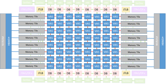
Coyote currently can model an architecture with a private L1 cache (data and instruction) and a shared banked L2 cache. The simulator allows to configure the size and the associativity of the L2 cache, and also the number of in-flight misses and the hit/miss latencies. Regarding the data mapping policies, Coyote supports page to bank (P2B) and set interleaving (SI). These features allow modeling simple tiled systems, including their L2s, implementing different sharing modes and data mapping policies, scalar cores and VPUs. In the ACME architecture, this corresponds to one VAS Tile component.
However, Coyote has evolved along these months and now several additional features have been added to enable a more accurate modeling of exascale systems. These can be grouped into 3 key areas, which match the most relevant components in the ACME accelerator: the VAS Tile, the Memory Tile and the Network-On-Chip interconnecting them. Thus, nowadays, Coyote is able to simulate more complex architectures. More specifically, regarding ACME accelerator, Coyote is able to simulate the architecture depicted below, whereas the shadowed boxes represent the unsupported architectural components.
The ACME architecture provides the high-level specifications of the accelerator, whereas the RTL design is responsible for designing and implementing the low-level details of the accelerator, being sure that the final design complies with the architectural specifications.
Before Coyote can start working, it needs to receive the specifications of the ACME accelerator, since they are used to model its underlying architecture. Once Coyote produces results, these are disseminated to both teams (Architecture and RTL). On the one hand, results obtained using Coyote might help to substantiate or reconsider architectural decisions. In any case, the information permits enhancing the architecture in early stages of the digital design cycle. On the other hand, the analysis of the design space exploration of ACME at simulation level provides clues and insights about the behavior of the architecture to the RTL design.
3. ACME as an emulated accelerator
The developed design, which plays the role of an emulated accelerator, will be a scaled-down version of ACME - small enough to fit in the FPGA, but big enough to test and validate the expected performance improvement of the ACME accelerator when it executes different kinds of HPC applications with dense and sparse workloads. This scaled-down version will include some number of VAS Tiles (interconnected among using a mesh topology NoC), and Memory Tiles. The number of final instances of each of these components will be dependent on two main factors: (1) the size of each developed component in terms of resources, and (2) the reserved resources on the FPGA-based emulation platform for the emulated accelerator (EA).
The ACME emulated accelerator development follows an incremental bottom-up approach, starting by working on the minimal computational components of the accelerator (block level), and then integrating them to build up more complex structures in the architectural hierarchy (system level, and then SoC level). Currently, two main components are in place: (1) a VAS Tile core, and (2) a VAS Tile.
VAS Tile core
A VAS Tile core is the minimal computational component, at system-level, which integrates several components: a scalar core, a vector processing unit, a specialized systolic array for video processing, and a specialized systolic array for neural network inference.
Both systolic arrays have the same interfaces: (1) control interfaces with the scalar core through OVI, and (2) data interfaces to read/write data from/to the scratchpad. In order to encapsulate the complexity of each of the systolic arrays, and deal with the interfaces, a common wrapper has been developed, named as SA-Shell.
The current status of this component is explained in the following video: Demo
VAS Tile
A VAS Tile is composed of a collection of VAS Tile cores and a shared L2 cache. The final amount of VAS Tile cores per VAS Tile will depend on the FPGA resources availability. However, in simulation different scenarios are being considered by parameterizing the system: number of vector lanes in the VPU, number of VAS Tile cores, size of the L2 cache.
The VAS Tile development is an iterative process, where each iteration adds more complexity and features to the component. A first approach to the VAS Tile has used OpenPiton as a scalable NoC system, using Ariane as a scalar core. The following one uses a Lagarto processor as a scalar core; and the next includes the support for executing vector instructions by adding a VPU.
Find more information about the VAS Tile approach in the following video: Demo
Find more information about the different components of the ACME accelerator in the following links: