As explained on MEEP’s platform ecosystem, the project extends the traditional accelerator system architecture beyond the traditional CPU-GPU systems by presenting a self-hosted accelerator. This accelerator is being conceived to improve HPC applications execution by running both, sequential and parallel code. It is also prepared to run some of the OS code.
The result is that:
- Data for the calculations can reside in the accelerator memory and does not have to be copied or marshalled to/from the host CPU memory to/from the accelerator.
- The system can benefit from a reduction in the host CPUs in the system.
- The increase of the number of accelerators “managed” by a traditional host leads to reducing the host CPU energy tax and boosting the system efficiency.
- It leverages economies of scale and technology advances driven by mobile chips to increase density and energy efficiency.
The MEEP project emulates an accelerator that in 5 years will be committed to a chiplet. The Accelerated Compute and Memory Engine (ACME) reflects the desire to improve the performance of dense and memory-bandwidth bound sparse workloads. Keeping this in mind, MEEP’s project is faced by following an incremental complexity development process; in which it is possible to distinguish two development and implementation phases:
- Phase 1. The initial focus is on a single EA and creating the infrastructure to run simple programs.
- Phase 2. The final target is being able to demonstrate a multi-EA implementation comprising several FPGAs, running more complex HPC software applications.
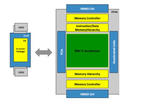
More specifically, the heart of MEEP is its emulation accelerator architecture, which is structured into two well-differentiated parts (Figure 1):
- The FPGA Shell: It contains all the necessary mechanisms for the accelerator to communicate with the host, and also with other neighboring accelerators.
- The Emulated Accelerator (EA): It is where all the data is processed and involves computation and memory management. In the future, MEEP will enable third parties to map their structures, accelerators, processors, etc., to the FPGA infrastructure. Initially, as a Proof of Concept (PoC), MEEP demonstrates its first accelerator architecture, the Accelerated Compute Memory Engine (ACME), as a collection of RISC-V IPs connected to a hierarchical memory structure.
A high-level description of the Emulated Accelerator: ACME
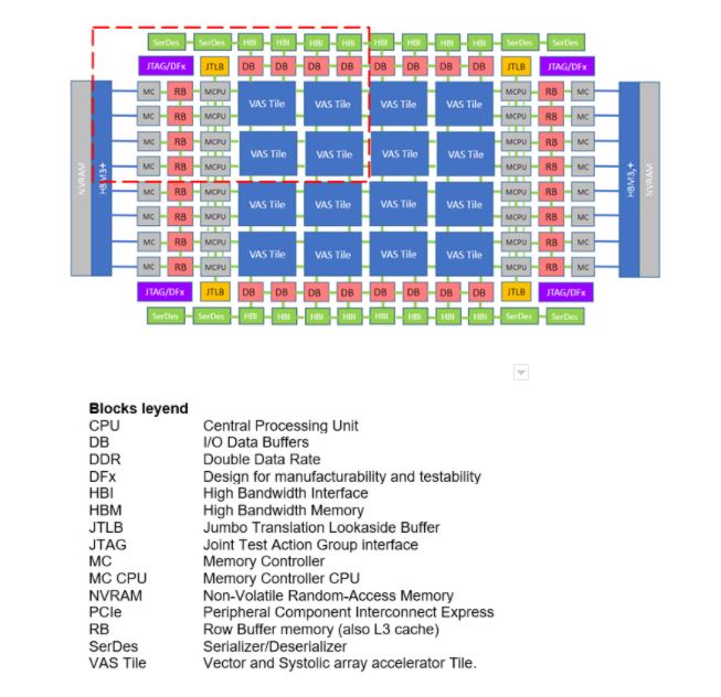
According to its name, the ACME architecture is composed of two main kinds of components: memory, and computational engines.
Memory components are distributed around these computational engines, getting as a result a complex memory hierarchy (from HBM and the intelligent memory controllers down to the scratchpads, and L1 caches), to move data and instructions from/to memory to/from the computational engines. In general, this memory distribution is a combination of software and hardware managed memory structures that enable high performance and energy efficiency. More in detail, the memory management and orchestration is under the Memory Controller CPUs or MCPUs responsibility.
The computational engine is a RISC-V accelerator, in which its main computational unit is called VAS (Vector And Systolic) Accelerator Tile. These units are instantiated multiple times and connected to each other with a NoC, and also connected to the memory elements.
Figure 2 shows the high-level ACME architecture with a variety of different major blocks.
Current work: Emulation Platform architecture: ACME (Phase 1)
The goal of MEEP in this phase is to capture the essential components of one of the chiplets in the FPGA and replicate that instance multiple times, a one-to-one mapping of an emulated accelerator to an FPGA. Consequently, this phase focuses its efforts on the first development of ACME (Accelerated Compute and Memory Engine -ACME).
ACME provides a grid of tiles of accelerators for HPC, HPDA, and video image processing. Within each tile, there are multiple scalar processors with associated coprocessors. Unlike normal accelerators or CPUs, a memory coprocessor has been included and moved close to the memory controller, creating a disaggregated architecture.
The core of the self-hosted accelerator is the VAS Tile, which is composed of a cluster of 8 computational cores. Internally, each core is directly connected to two computational coprocessors: a Vector Processing Unit (VPU) and a Systolic Array (SA). Actually, there is an extra memory coprocessor (MCPU) that resides near the memory controllers of the HBM memory which is more VAS Tile related, but that impacts on each core too.
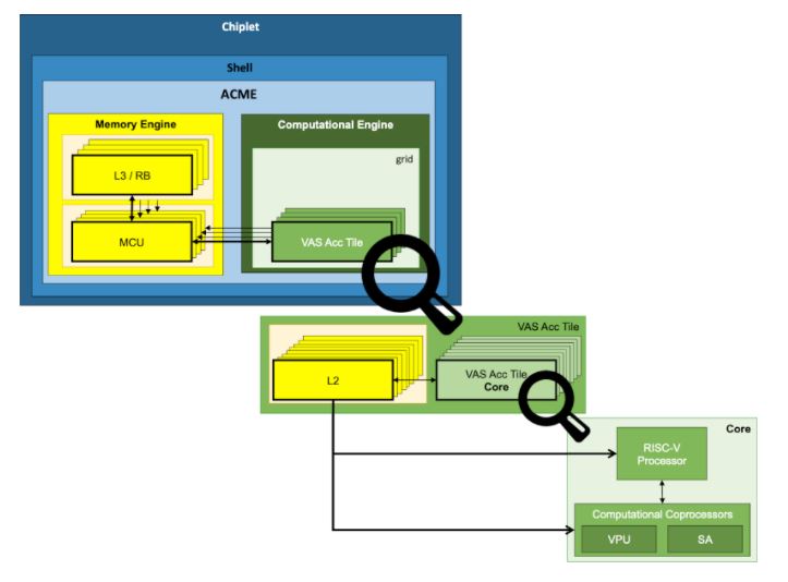
All the cores within a VAS Accelerator Tile share an L2 data cache that is 4 MB in size with 16-ways and 16 banks. This shared resource brings the flexibility of acting as a scratchpad by disabling cache ways in the L2.
Each MCPU, as a memory coprocessor, can also operate on vector index registers for scatter/gather operations and memory operations like atomics and simple arithmetic operations. MCPUs are overprovisioned in the accelerator to have enough computing capabilities left to run the local OS, daemons, and other resource scheduling and accounting software. This increases the self-hosting capabilities of the ACME accelerator.
This architecture also supports an L3 cache that can also function as a DRAM row or page buffer. If there is significant reuse of data in the row buffer, it can be stored on-chip and act as a DRAM row buffer creating a higher dimension virtually interleaved DRAM. The row buffer (re)placement policies as well as many other HBM and on-chip memory policies are controlled and informed by the Memory Controller (MC) CPU.
Computational Coprocessors
The computational coprocessors, under the RISC-V core control, have the purpose of accelerating the execution of HPC applications by exploiting significant data-level parallelism inherent to SIMD architectures.
There are two kinds of coprocessors in a VAS Accelerator Tile Core:
- Vector Processing Unit (VPU): This block is able to process a whole vector simultaneously, which means multiple data at the same time.
- Systolic Arrays (SA): This block is able to process streams of data. As part of their behavior, these SA reuse the same data multiple times internally to fulfill with close data dependencies.
The instruction stream is processed by the scalar core and coprocessor instructions are forwarded to the appropriate unit, similar to the old MIPS systems and other systems. In ACME, this is extended to include memory instructions as dedicated coprocessor instructions. The dedicated memory coprocessor is moved to the memory controller vs being located in the core. This enables a lot of the accelerator memory operations like address generation to be collocated with the memory coprocessor.
Both Computational coprocessors, the VPU and the SA are computationally independent of each other but connected to the same RISC-V processor. Figure 4 represents the interfaces of these coprocessors and some details of the VPU.
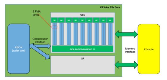
Vector Processing Unit (VPU)
The proposed VPU extends the capabilities of the EPI [EPI] vector unit, connected to a scalar processor via an open vector interface [OVI], and with its own memory interface to the shared L2 cache. Internally, it also has 16 vector lanes, which can be subdivided down to 2 lanes and mapped to threads. Multiple powers of two lanes (2, 4, 8, or 16) can be fused together and supported by a single thread, as well. The associated scalar core can support up to 8-way coarse-grain multithreading (CGMT) to support the lane configuration. At a higher-level, dense HPC computations will be supported by a fully fused VPU, whereas sparse computations rely on multiple outstanding misses, which the 8 threads can issue and be supported by 2-lane VPUs, given VPU throughput is less of an issue compared to memory bandwidth limitations.
The VPU in MEEP, in the image above, highlights two more aspects to consider. On one hand, there is not a unique vector Register File (VRF) but broken into smaller and reduced length VRFs to support one lane pair each. On the other hand, the VPU improves the communication capabilities between the lanes and also map functions to the interlane communication like sorting, reductions, and other simple arithmetic operations.
Systolic Arrays (SA)
Systolic Arrays (SA) provide efficient mechanisms for processing a variety of data, from image and video processing to neural networks. Like the VPU, the SAs require some management, as well as access to memory; which are provided through the same interfaces as the VPU. The scalar core provides the control and orchestration of the SA, and the L2 scratchpad provides the streaming memory interface to the SA to enable sustained high performance.
To support different kinds of applications, MEEP proposes a common SA Shell template for all of them. This template fixes the interfaces with the scalar processor and memory, but the final internal structure of the computational block will depend on the nature of the application to be executed. Particularly, MEEP is focused on two very demanding applications, one for encoding/decoding the HEVC [HEVC] video standard, and another one for Neural Networks.
References
[OVI] Open Vector Interface (September 2020): https://github.com/semidynamics/OpenVectorInterface
[EPI] European Processor Initiative: https://www.european-processor-initiative.eu/
[HEVC]: https://www.itu.int/rec/T-REC-H.265
For more information about MEEP's next steps in the near future, visit MEEP’s platform ecosystem section.